True to Moore’s Law, the number of transistors on a microchip has doubled every year since the 1960s. But this trajectory is predicted to plateau soon as silicon – the backbone of modern transistors – loses its electrical properties when devices made of this material fall below a certain size.
Enter 2D materials — delicate, two-dimensional sheets of perfect crystals that are as thin as a single atom. At the nanometer scale, 2D materials can conduct electrons much more efficiently than silicon. The search for next-generation transistor materials has therefore focused on 2D materials as potential successors to silicon.
But before the electronics industry can transition to 2D materials, researchers must first find a way to engineer the materials on industry-standard silicon wafers while preserving their perfect crystalline shape. And MIT engineers may now have a solution.
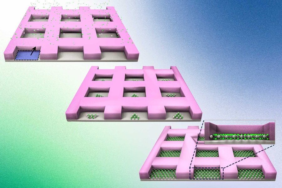
By depositing atoms onto a wafer coated in a “mask” (top left), MIT engineers can corral the atoms into the mask’s individual pockets (middle center) and encourage the atoms to grow into perfect, 2D, single-crystalline layers (bottom). Right).
Acknowledgments: Courtesy of the researchers. Edited by MIT News.
The team has developed a method that could enable chipmakers to make ever-smaller transistors from 2D materials by growing them on existing wafers of silicon and other materials. The new method is a form of “non-pitaxial, single-crystalline growth”, which the team used for the first time to grow pure, defect-free 2D materials on industrial silicon wafers.
Conducts electricity better than silicon
Using their method, the team fabricated a simple functional transistor from a type of 2D material called transition metal dichalcogenides, or TMDs, which are known to conduct electricity better than nanometer-scale silicon.
“We expect that our technology can enable the development of 2D semiconductor-based, high-performance, next-generation electronic devices,” said Jeehwan Kim, associate professor of mechanical engineering at MIT. “We’ve unlocked a way to catch up with Moore’s law using 2D materials.”
Kim and his colleagues describe their method in a paper appearing today in Nature. The study’s MIT co-authors include Ki Seok Kim, Doyoon Lee, Celesta Chang, Seunghwan Seo, Hyunseok Kim, Jiho Shin, Sangho Lee, Jun Min Suh, and Bo-In Park, along with collaborators at the University of Texas at Dallas, the University of California at Riverside, Washington University in Saint Louis and institutions across South Korea.
A crystal patchwork
To produce a 2D material, researchers have typically used a manual process in which an atomically thin flake is carefully exfoliated from a bulk material, like peeling away the layers of an onion.
However, most bulk materials are polycrystalline and contain multiple crystals growing in random directions. Where one crystal meets another, the “grain boundary” acts as an electrical barrier. Any electrons flowing through a crystal stop abruptly when they meet a crystal with a different orientation, dampening a material’s conductivity. Even after exfoliating a 2D flake, the researchers must search for “single-crystalline” regions—a tedious and time-consuming process that is difficult to apply on an industrial scale.
Recently, researchers have found other ways to make 2D materials, by growing them on wafers of sapphire – a material with a hexagonal pattern of atoms that encourages 2D materials to assemble in the same single-crystalline orientation.
2D materials on silicon
“But no one uses sapphire in the memory or logic industry,” says Kim. “All infrastructure is based on silicon. For semiconductor processing, you have to use silicon wafers.”
However, wafers of silicon lack the hexagonal support structure of sapphire. When researchers try to grow 2D materials on silicon, the result is a random patchwork of crystals that fuse together at random, forming many grain boundaries that hinder conductivity.
“It is considered almost impossible to grow single-crystalline 2D materials on silicon,” says Kim. “Now we show you can. And our trick is to prevent the formation of grain boundaries.”
Seed pockets
The team’s new “non-pitaxial, single-crystalline growth” does not require the scaling and searching of flakes of 2D material. Instead, the researchers use conventional vapor deposition methods to pump atoms across a silicon wafer. The atoms eventually settle on the disk and form nuclei and grow into two-dimensional crystal orientations. If left alone, each “nucleus” or seed of a crystal would grow in random orientations across the silicon wafer. But Kim and his colleagues found a way to align each growing crystal to create single-crystalline regions across the entire disc.
To do so, they first covered a silicon wafer in a “mask”—a coating of silicon dioxide that they patterned into tiny pockets, each designed to trap a crystal seed. Over the masked disk, they then flowed a gas of atoms that settled into each pocket to form a 2D material—in this case, a TMD. The pockets of the mask held the atoms together and encouraged them to assemble on the silicon wafer in the same single-crystalline orientation.
Made a simple TMD transistor
“It’s a very shocking result,” says Kim, “You have single-crystal growth everywhere, even though there is no epitaxial relationship between the 2D material and the silicon wafer.”
Using their masking method, the team fabricated a simple TMD transistor and showed that its electrical performance was as good as a clean flake of the same material.
They also applied the method to construct a multilayer device. After covering a silicon wafer with a patterned mask, they grew one type of 2D material to fill half of each square, then grew a second type of 2D material over the first layer to fill the rest of the squares. The result was an ultra-thin, single-crystalline bilayer structure within each square. Kim says that going forward, multiple 2D materials can be grown and stacked together in this way to make ultra-thin, flexible and multifunctional films.
US Defense Advanced Research
“Until now, there has been no way to make 2D materials in single-crystalline form on silicon wafers, so the whole community has struggled to realize next-generation processors without transferring 2D materials,” says Kim. “Now we have completely solved this problem, with a way to make devices smaller than a few nanometers. This will change the paradigm of Moore’s law.”
This research was supported in part by the US Defense Advanced Research Projects Agency, Intel, the IARPA MicroE4AI program, MicroLink Devices, Inc., ROHM Co. and Samsung.
#MIT #engineers #grow #perfect #atomically #thin #materials #industrial #silicon #wafers